FIB/SEM - FEI Helios G4 PFIB CXe dual beam - Status: Available
|
*ANALYSIS OF RADIOACTIVE SPECIMENS WITH THIS INSTRUMENT IS STRICTLY PROHIBITED*
PLEASE NOTE: published rates are for the first 8 hours of usage; the rates then decrease as specified below (runs not to exceed 24 hours in total):
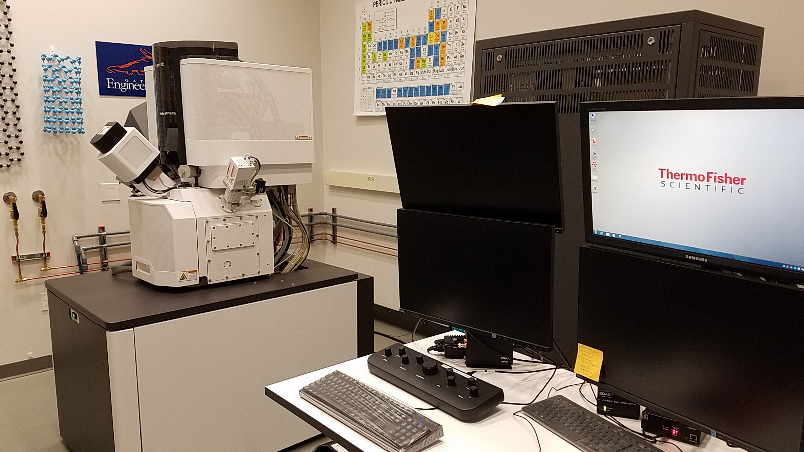
The FEI Helios G4 PFIB CXe DualBeam system integrates focused ion and scanning electron beams for FIB and SEM functionality in one instrument. Instrument Specifications: Virtual workshop: dual FIB/SEM tips, tricks, and other useful info (11/19/21) YouTube tutorial: EBSD using EDAX Velocity EBSD camera and TEAM software (08/24/22) YouTube tutorial: dual PFIB/SEM for S/TEM lamella preparation (03/03/23) EDAX webinar: introduction to EBSD (10/03/23) EDAX webinar: post-processing of EBSD data (02/02/22) EDAX webinar: optimizing EBSD results using OIM 8 (02/22/22) YouTube tutorial: dual PFIB/SEM for in-situ UHR SEM imaging of PFIB-prepared cross-sections (04/13/24) YouTube tutorial: dual PFIB/SEM for S/TEM lamella preparation (02/11/25) YouTube tutorial: EBSD + EDS using EDAX Velocity EBSD, Octane Elite EDS, and APEX software (02/24/25) TRAINING REQUIREMENTS: 1. Please create an NRF user account with a PI-approved funding source. 2. Please complete NRF general safety training. 3. Please complete the FIB Knowledge Training course through eLearning; submit a training request using the "Training" link at the bottom of the page and follow the instructions to be added to the course; you must complete this course regardless of any prior coursework or operational experience related to SEM or FIB you may have. |
- Ga-free S/TEM lamella preparation via in-situ lift-out method
- Rapid, large scale (>100 um) cross-section face preparation
- High-resolution (<1 nm) top-down and cross-sectional SEM imaging
- Nanoscale (<100 nm) to microscale (>1 um) electron and ion beam-assisted milling, patterning, and deposition
- Automated serial sectioning and cross-section face imaging
- Nanoscale (<100 nm) to microscale (>1 um) compositional analysis using EDS
- Nanoscale (<100 nm) to microscale (>1 um) texture and crystallographic analysis using EBSD
An active Gatorlink login is required to create a new reservation.